Our Mission
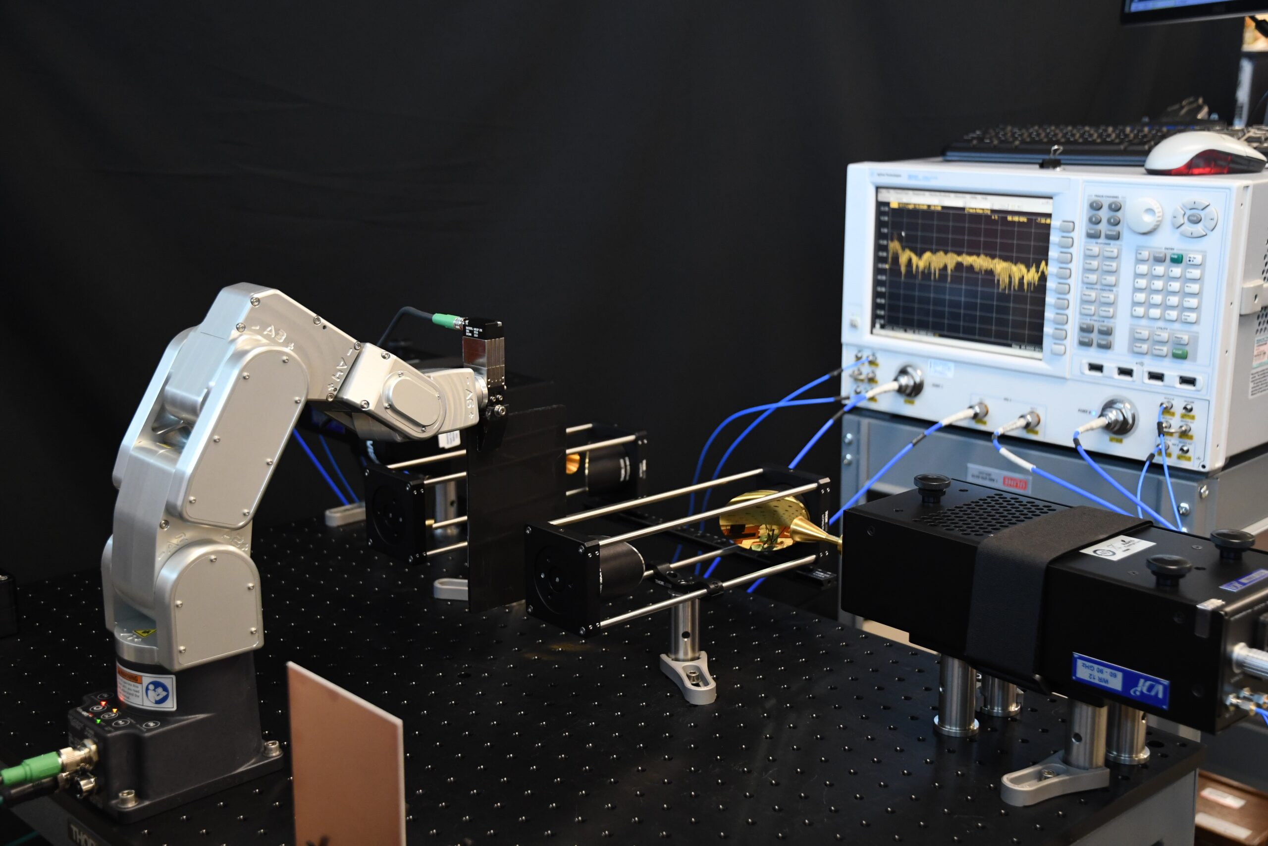
Provide an effective alternative to contact-probes for on-wafer characterization of high-speed devices and Integrated Circuits (ICs). Our approach is very different from the current norm: Instead of making physical contact to launch and receive test signals, we use highly-focused high-frequency beams and tiny on-wafer antennas to eliminate the physical contact between the test system and the device under test. No contact means no wear & tear and absolutely no need for fragile contact probes. Our approach eliminates contact-repeatability that plague the measurements and require an extremely-expensive rig to overcome. By eliminating the vertical motion required for making contact with the test wafer, our systems enable fully-automated periodic calibration and unattended characterization of entire wafers without user intervention.
TeraProbes patented high-frequency test-bed (probe station and proprietary single-ended and full-differential-mode probes) enables automated, industrial-scale testing of electronic device and ICs without making physical contact to the wafer. A single rig provides the user with coverage from 50GHz-1.1THz and beyond, for single-ended (e.g. co-planar waveguide) and full-differential mode characterization over the entire 50GHz-1.1THz band and beyond.
Our History
We started TeraProbes, Inc. in 2014 as a spin-off from our research at the Electrical and Computer Engineering Department at The Ohio State University. We believe our non-contact probing technology can help alleviate pains in the high-speed electronics industry associated with contact probe wear & tear, contact repeatability, and extremely-high hardware and operation costs associated with on-wafer device and IC characterization.